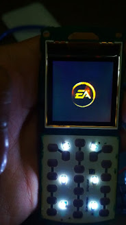
Photo by : Subhankar Karmakar
Month Selector - Click to see posts from a particular month only
Sunday, May 17, 2020
Saturday, May 16, 2020
Photo by : Subhankar Karmakar
Theme : Technology - Taking Closeup pictures of pixels of the display using a manual focus web cam
Thursday, May 14, 2020
Photo by : Subhankar Karmakar
Theme : Technology - Opening a phone and taking external power supply to know how every small component works
Tuesday, May 12, 2020
Photo by : Subhankar Karmakar
Theme : Technology - Opening a phone and taking external power supply to know how every small component works
Photo by : Subhankar Karmakar
Theme : Technology - Opening a phone and taking external power supply to know how every small component works
Tuesday, May 5, 2020

I have used photos from my mobile and some old junk hard disk controller PCBs and other junk PCBs, anyways I have designed one but have not got it manufactured, and for softwares I have used KiCAD – it is free software and you can get it and run it easily and also I have used images from Altium designer software( it is not free ) & Autodesk EAGLE. There is this prominent software which is completely online and is linked with an assembler called the EasyEDA and you can try it too ! Also for KiCAD example and many demo files we have many repositories on internet from OSH-park and other open source hardware companies which give out free complex PCB design files.
In future posts I will try to make a comparison between this PCB manufacturing and IC fabrication !
Monday, May 4, 2020
Now that we have designed our PCB we just now have to get the design files exported and get a almost standard output file that a manufacturer will understand and will translate them into good looking PCB. So well there are export options in design softwares which can export the PCB design file in a format called GERBER format and NCDRILL files which then can be submitted online and an order can be placed at PCB manufacturing web sites.
Now during placing orders also we have a lot of options to choose and one of them is solder mask colour and silk screen colour, now what these two are they are just as we see them, the solder mask colour is the colour of the PCB that is we see green coloured PCB, blue coloured PCB and the markings on them or writings on them are mostly done using white and they are called silk screen colour, the most prominent and most widely seen PCB are green coloured PCB with white text written on them and manufacturing them also cost less.
Later after the PCB gets manufactured and you get in your home then the placing of components will come and the use of solder mask will be prominent as it helps you exposing the contact pads and helps you solder properly without sorting the existing copper contacts and tracks.
The silk screen tells us where to place the components.
Also there is auto assembly offered by many PCB manufacturers and we can pay them so that they buy our components and assemble them using pick and place machines, more about them later !
Blog Archive [Please go through posts from top to bottom so as to make sence of the big picture]
-
▼
2020
(40)
-
▼
May
(8)
- From copper to PCB [Part 7] – Placing an order for...
- From copper to PCB [Last Part] – Photos I have use...
- Compact Disks
- Random Photographs by Subhankar [Opening a phone a...
- Random Photographs 002 by Subhankar [Opening a pho...
- Random Photographs 003 by Subhankar [Opening a pho...
- Random Photographs 004 by Subhankar [Taking Closeu...
- Random Photographs 005 by Subhankar [Opening a pho...
-
▼
May
(8)
About our Original Photographs
All the Photograph Posts are original and belongs to this blog, Do not use them without credits or mentioning that they are from this blog or who shot the original picture.


