Here's a very crude analogy to explain the difference between analog and digital sound, a vinyl records walls generate an analog signal by moving the stylus left and right as well as up and down its diagonally moved for stereo, but just imagine for a moment that it's just left and right a record directly. That's the analog signal via the motion of the stylus.

But a digital Sound Source is instead sort of like a virtual stylist riding in a virtual Groove. The sound samples are snapshots in time of where the stylist was a DAC will then create an analog signal by running a virtual stylist through this virtual Groove and placing it at exactly the correct location and thus generating the appropriate voltage level as defined by the samples by using a giant list of numbers to recreate sound instead of the Local properties of a plastic disc the sound can be reproduced flawlessly and accurately with no Reliance on the record players cartridge properties. The Integrity of its stylus. It's motor the quality of the vinyl Etc.
The biggest Boon of digital sound was that it eliminated all of the little nuances that might change how a recording sounds digital sound is in a sense absolute but getting digital sound into the hands of the average consumer took a long. It's the amount of raw data generated by sound recording was immense for the standards of the time although 650 megabytes. The data equivalent of the first compact discs is a paltry sum of data in the 21st century.
It was unimaginably huge in the early 1970s when the first commercial digital sound recording took place for context the Commodore 64 released the same year as the compact disc has 64 kilobytes of RAM and that was considered huge for the time a compact disc held Roughly 10,000 times as much data 64 kilobytes of cd-quality audio lasts this long that's not super helpful.
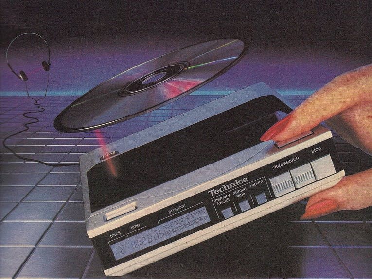
We will continue to look at the methods that were used to store data from digital recordings and we'll discuss the rise of the compact disc as a robust consumer friendly format for digital sound reproduction and distribution.


![Mediatek System on Chip[MT6582] next to the ROM of Micromax Q380](https://blogger.googleusercontent.com/img/b/R29vZ2xl/AVvXsEg9HOisCjakFJDZ9PoIlioAUTOFH7n0_kCqIcDkLJ9KXkdBFEzDihnA-gw08KW_xrb6ELRjHnlu6fe3rdmtaUbzoWLXseLCHoFfKqVaPLVAKvzqPP_r_g69sQ3jaq5DjWLUMBqFQCOnQVtE/s263/a92ac451a7800d5d712cbaa834d5d98d.jpg "Mediatek System on Chip[MT6582] next to the ROM of Micromax Q380")


")
")


