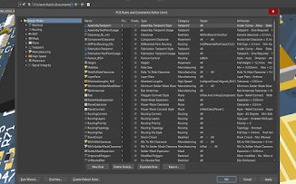
Now as we have said about routing tracks, we have to understand that this track placing or routes and via have rules that is the manufacture can only make them physically in a certain way we cannot draw and demand something which is lets say very small and very close placing of copper tracks or components as you have to understand there are physical machines, etching solutions, copper depositors which will work at some point of time on your designed PCB and they have some very real physical and practical limitations which are inevitable.
So, we cannot place copper tracks too close, we cannot place components too close, we cannot make via too close or close to a drill point. We cannot drill too close and so on. Also due to this there are auto routers which help in taking this DRC in account and the software or the algorithm or the computer as we see can just place or draw the tracks all by itself and there is just no need to worry about breaking rules and creating huge trouble.
So in this way our PCB design gets completed. I know this is not a very detailed explanation but it is something or the series is something that can at least give you a rough idea about what is happening.


0 comments:
Post a Comment