Photo by : Subhankar Karmakar
Theme : Technology - Opening a phone and taking external power supply to know how every small component works


Photo by : Subhankar Karmakar
Photo by : Subhankar Karmakar


Photo by : Subhankar Karmakar


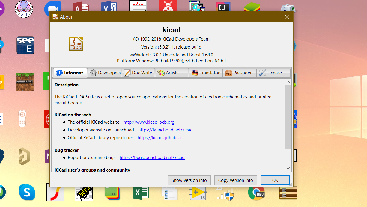
I have used photos from my mobile and some old junk hard disk controller PCBs and other junk PCBs, anyways I have designed one but have not got it manufactured, and for softwares I have used KiCAD – it is free software and you can get it and run it easily and also I have used images from Altium designer software( it is not free ) & Autodesk EAGLE. There is this prominent software which is completely online and is linked with an assembler called the EasyEDA and you can try it too ! Also for KiCAD example and many demo files we have many repositories on internet from OSH-park and other open source hardware companies which give out free complex PCB design files.


Now that we have designed our PCB we just now have to get the design files exported and get a almost standard output file that a manufacturer will understand and will translate them into good looking PCB. So well there are export options in design softwares which can export the PCB design file in a format called GERBER format and NCDRILL files which then can be submitted online and an order can be placed at PCB manufacturing web sites.


Now during placing orders also we have a lot of options to choose and one of them is solder mask colour and silk screen colour, now what these two are they are just as we see them, the solder mask colour is the colour of the PCB that is we see green coloured PCB, blue coloured PCB and the markings on them or writings on them are mostly done using white and they are called silk screen colour, the most prominent and most widely seen PCB are green coloured PCB with white text written on them and manufacturing them also cost less.
Later after the PCB gets manufactured and you get in your home then the placing of components will come and the use of solder mask will be prominent as it helps you exposing the contact pads and helps you solder properly without sorting the existing copper contacts and tracks.
The silk screen tells us where to place the components.
Also there is auto assembly offered by many PCB manufacturers and we can pay them so that they buy our components and assemble them using pick and place machines, more about them later !


Now as we have said about routing tracks, we have to understand that this track placing or routes and via have rules that is the manufacture can only make them physically in a certain way we cannot draw and demand something which is lets say very small and very close placing of copper tracks or components as you have to understand there are physical machines, etching solutions, copper depositors which will work at some point of time on your designed PCB and they have some very real physical and practical limitations which are inevitable.


So, we cannot place copper tracks too close, we cannot place components too close, we cannot make via too close or close to a drill point. We cannot drill too close and so on. Also due to this there are auto routers which help in taking this DRC in account and the software or the algorithm or the computer as we see can just place or draw the tracks all by itself and there is just no need to worry about breaking rules and creating huge trouble.


So in this way our PCB design gets completed. I know this is not a very detailed explanation but it is something or the series is something that can at least give you a rough idea about what is happening.

So for now we have only discussed about how the two layers are, but depending on the use case, there can be more than two layers and in that case the manufacturers have more copper sand witches sand witched and through our given GERBER information, what diagrams are to drawn on sides are conveyed and all are drawn independently and then sand witched.

Now I have said there are files which convey information, so
I have a point to add that these all assembly are done in parts and only the
diagram part and drill parts are done with the help of drill machines and photo
developers and oxidation and copper deposits etc.


Now as we sort of now know how the PCB is manufactured lets
start where we left off, that is after logical diagram and attaching
footprints.

So, after all those we just have to draw circuits and those
are just how copper tracks will go where the components will be placed, where
the power lines will be where the ground planes will be and so on. Also first
we just have to place components in place as we want and they are connected
with the help of raster nets which are derived from the logical diagram
actually, and these raster nets are then to be made copper tracks that is how
physically copper will run from one component to another and how the ground
planes would be. These running of copper tracks is called routing and has some
specific rules.

So, after we have done logical schematic diagram with footprints attached we can now just start drawing on the PCB using our softwares Physical layout editor or a board designer, here what we draw initially is on the top surface of the PCB.

Ok so as I have said surface and we are into physical view
now so lets describe how physically the PCB is prepared in the real world in
fabrication centre. So, in fabrication centre they start with something called
a copper sandwich, which is copper layers on either side with a dielectric
material between them, the dielectric material is what the whole PCB gets
support on and the top and bottom sides are copper so all the electrical
diagrams and contacts and contact pads and via are done on them using first
marking with help of UV and then etching.
So, first the raw material as described is taken and then
the diagrams from the customer are taken and transferred on the copper layers
as per given formats. Now for this transfer there is no specific PCB design
file, but as we might have heard of we have something called as GERBER files
which are files which are generated from the PCB design software and have all
the information about how the board drawings would be and how the silkscreen
that is all the writings and diagrams would be and how the copper pads will be
exposed after the solder mask and a NCDRILL file which tells where the
mechanical boundaries are and how the holes are to be drilled.


